S-9.1 デジタルコマンドコントロールの電気的標準
原文版:3/07/2020
デジタルコマンドステーションからデジタルデコーダーへの通信は命令を伝達する一連のビットを転送することによって成り立っています。ビットは2つの状況のうちの1つをあらわす信号であり、それを 1 と 0 とします。この章では、これらのビットを符号化する DCC 信号の電気的特性について記述します。Please refer to tables 1-32 for definition and numerical values of parameters used throughout this document.
A:ビットを符号化する方式
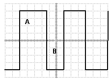
NMRA DCC 信号の基本は反対の極性をもつ連続した2つの電圧レベルの遷移です1。交互に起こる遷移がビットを次のビットと分割します。残りの遷移がそれぞれの部分を前半と後半に分割します。デジタルコマンドステーションは、ビットの期間つまり遷移の周波数を変化させることによって DCC のこの連続した遷移にビットを符号化します。
1 ビットでは、ビットの前半と後半で名目上同じ期間となり、それを 2 とします。よってビット全体の期間は です。デジタルコマンドステーションは、前半と後半のそれぞれが の期間をもつように 1 ビットを送信しなければいけません。 1 ビットの前半と後半の期間の差は を超えてはいけません。デジタルデコーダーは、前半と後半の期間の期間が の範囲内なら 1 の値をもつ妥当なビットとして受け付けなければいけません。デジタルデコーダーは、正と負の部分の期間の差が を超えない場合、 1 ビットとして受け付けなければいけません。
0 ビットでは、それぞれの遷移の前半と後半の期間は名目上 と等しいかそれより大きくないといけません。 1 ビットと同じように信号全体における直流値を0にするため 0 ビットの前半と後半も一般的には等しい期間です。デジタルコマンドステーションは、ビットのそれぞれの部分が 以内の期間をもつように、また 0 ビットの全期間が を超えないように 0 ビットを送信しなければなりません。デジタルデコーダーは、前半か後半が 以内の期間をもつビットを 0 の値をもつ妥当なビットとして受け付けなければいけません。Figure 1 provides an example of bits encoded using this technique.

これは接地のない差分信号です。信号線が水平基準線と交叉するという点において、両方の線路は等しい電圧となります。
1ビット計時
負荷時のパワーステーションの出力は下記です。
| 1ビットの関係 | 結果 |
|---|---|
| または | 不可 |
| 可 | |
| 可 | |
| 不可 |
デコーダーは下記を受け付けなければいけません。
| 1ビットの関係 | 結果 |
|---|---|
| かつ | 可 |
| 可 | |
| 可 |
| 変数 | 定義 | 最小値 | 通常値 | 最大値 | 単位 | 備考 |
|---|---|---|---|---|---|---|
1 の半ビット期間 |
55 | 58 | 61 | μ秒 | 1 の半ビットの転送継続時間 |
|
1 の半ビット受信期間 |
52 | 58 | 64 | μ秒 | 受信した 1 の半ビットの許容期間 |
|
0 の半ビット期間 |
95 | 100 | 9900 | μ秒 | 0 の半ビットの転送継続時間 |
|
0 ビットの伸張期間 |
— | — | 12000 | μ秒 | 引き伸ばされた 0 ビットの最大総和継続時間 |
|
0 の半ビットの受信期間 |
90 | 100 | 10000 | μ秒 | 受信した 0 の半ビットの許容期間 |
|
1 の半ビット期間の差分 |
— | — | 3 | μ秒 | 転送した 1 の半ビットの期間の最大の差 |
|
受信した 1 の半ビット期間の差分 |
— | — | 6 | μ秒 | 受信した 1 の半ビットの期間の最大の差 |
B:コマンドコントロール信号の形
デジタルコマンドコントロールシステムによって線路に適用された NMRA 信号は、パワーステーションの出力を無負荷から電力源の許容する最大連続負荷までの条件下で計測すると、下記の特性をもつ必要があります。Transitions that cross the region between and 3 shall occur at the rate of VtrA or faster. This signal may contain non-monotonic distortion at the zero-crossing transitions, provided that this distortion shall have an amplitude of no greater than 4.
Digital Decoders shall be designed to correctly decode signals with transitions whose slope is or faster across the voltage range from to . A Digital Decoder shall correctly decode properly addressed baseline packets at a probability of or higher, as defined in S-9.2, in the presence of noise (and/or other types of signals) at frequencies above with a total peak-to-peak amplitude of less than () of the peak-to-peak amplitude of the NMRA digital signal5.
The exact shape of the NMRA digital signal shall be designed to minimize electromagnetic radiation such that a large layout operated using this standard can meet applicable United States Federal Communications Commission electromagnetic interference requirements6.
| Parameter | Definition | Min. Value | Normal Value | Max. Value | Unit | Comments |
|---|---|---|---|---|---|---|
| Transition region | — | -4 | — | Volt | Low limit of bit transition region | |
| Transition region | — | 4 | — | Volt | High limit of bit transition region | |
| Transition rate | 2.4 | — | — | Volt/μsec | Transmitted bit voltage transition rate | |
| Distortion amplitude | — | — | 2 | Volt | Distortion voltage during bit transition | |
| Receive transition rate | 2 | — | — | Volt/μsec | Received bit voltage transition rate | |
| Decode probability | 95 | — | — | Percent | Percentage of packets decoded correctly | |
| Noise frequency | 100 | — | — | kHz | Frequency of noise or other signal | |
| Peak signal to noise amplitude ratio | 4:1 | — | — | No units this is a ratio |
Peak DCC signal to peak |
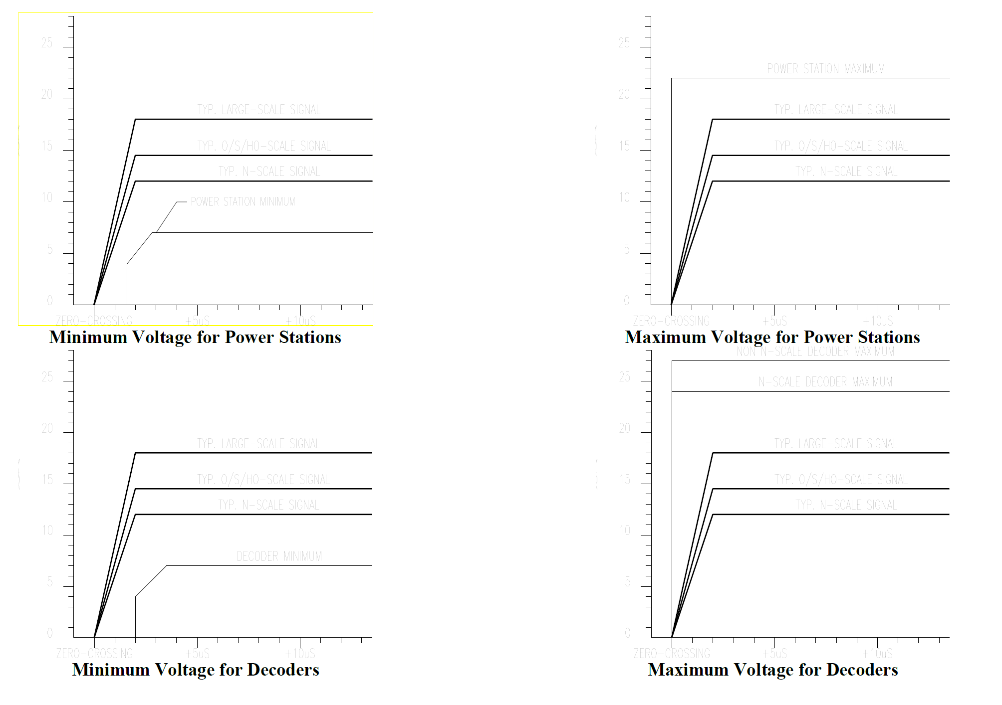
C: Power Transmission and Voltage Limits for Transmitting Power through the Rails
The baseline method for providing the power to operate locomotives and accessories, which shall be supported by all Digital Command Stations and Digital Decoders, is by full-wave rectification of the bipolar NMRA digital signal within the Digital Decoder7. In order to maintain power to the Digital Decoders, gaps in bit transmission are only allowed at specified times (see S-9.2, Section C). The peak value of NMRA digital signal, as produced by the power station and measured at the track, shall be confined to the range of for the applicable scale, as specified in Table 38. In no case should the peak amplitude of the command control signal exceed for the applicable scale.
Digital Decoders shall be designed to continuously operate in and withstand, without permanent damage to the decoder; a peak maximum voltage within the range of as specified in table 3 for the applicable scale, measured at the track.
| Scale | Parameter | Definition | Min. Value | Normal Value | Max. Value | Unit | Comments |
|---|---|---|---|---|---|---|---|
| N and smaller scales | Voltage limits for track for power station | 8.5 | 12 | 22 | Volt | Voltage produced powering the track | |
| HO/S/O scales | Voltage limits for track for power station | 8.5 | 15 | 22 | Volt | Voltage produced powering the track | |
| Large scales | Voltage limits for track for power station | 8.5 | 18 | 22 | Volt | Voltage produced powering the track | |
| N and smaller scales | Voltage limits for track for decoder | 7 | 12 | 24 | Volt | Peak voltage decoder should operate in and withstand | |
| HO/S/O scales | Voltage limits for track for decoder | 7 | 15 | 27 | Volt | Peak voltage decoder should operate in and withstand | |
| Large scales | Voltage limits for track for decoder | 7 | 18 | 27 | Volt | Peak voltage decoder should operate in and withstand |
Digital Decoders shall be designed to interpret a valid packet addressed to it whilst supplied a minimum voltage as specified in Table 3 and to acknowledge the receipt of a command in that packet by some action. E.G. turning on a low power output to illuminate an LED. The Digital Decoder is not required to turn the motor at this voltage. This is an indication of the Digital Decoder’s ability to read valid instructions addressed to it at the specified minimum voltage at the track.
| Data | Revisions |
|---|---|
| January 2019 | Tabularized data, removing it from the text and replacing with a variable to make future revisions less prone to missing changes in the text. Cleaned up grammar and language. |
| February 2019 | Table 3 increased large-scale power station maximum voltage large to 24v from 22v. |
| July-August 2019 | Text related to Table 3 to clarify the decoder must operate continuously in the maximum voltage specified without sustaining permanent damage. The decoder must read and acknowledge a valid instruction addressed to it at the minimum voltage specified. |
1. 機関車やいくつかの客車・貨車はそれぞれの方向に向いて線路に置かれるため、デジタルデコーダーからはビットの前半と後半のどちらが正の電圧になるか定義することは不可能です。 ↩
2. 全ての計測は0ボルトと交叉する区間を計測します。 ↩
3. 0 volts is the mid point of the differential voltage. ↩
4. This standard specifically permits super-imposing non-NMRA signals upon the rails for other purposes, provided that the NMRA Digital Decoder can reject these signals. ↩
5. This measurement is made with the Digital Decoder electrically connected to a track or accessory bus. ↩
6. All components of an NMRA compliant digital system shall meet all applicable FCC and/or CE requirements. ↩
7. Alternate means for supplying power are acceptable, provided that Digital Command Station power units are capable of producing the baseline track signal, and Digital Decoders are capable of operation from the baseline track signal as described by this standard. ↩
8. Care should be taken to ensure that any motors exposed directly to the digital signal for extended periods have a stall rating that exceeds the amplitude of the signal, or sufficiently high impedance at 4-9 kHz to reduce the current to normal operating level. This appears to only be a concern for high-precision core-less can motors, which present a low impedance load, or for layouts using an NMRA digital signal with an amplitude in excess of ± 18 volts. ↩